Exhibition
Invitation | Mikrouna invites you to participate in the 2022 Forum on the Development of Nanooptoelectronic Materials and Semiconductor Devices
2022-11-10
from:
Time and place of the meeting
Location: Beijing, China
Time: November 11 to November 13, 2022
Background
In order to boost the rapid development of China's nano optoelectronic materials and semiconductor devices and technologies, promote the exchange and cooperation of researchers and industry peers in the field of optoelectronic materials and devices, promote the rapid and healthy development of upstream and downstream industrial chains, further promote the in-depth cooperation of the industrial chain and the transformation of scientific and technological innovation achievements, the Nano Materials Expert Committee of the Optoelectronic Materials and Devices Network, the University of Chinese Academy of Sciences, and the China New Materials Development Platform Scientist Think Tank The semiconductor materials expert committee and the joint decision were made to hold the "2022 Nanometer Optoelectronic Materials and Semiconductor Devices Development Forum" in Beijing from November 11 to 13, 2022.
With the purpose of creating a high-level, high-quality and effective event, the "Nanooptoelectronic Materials and Semiconductor Devices Development Forum" invited many well-known experts at home and abroad to carry out multi angle, strategic and forward-looking research exchanges, focusing on optoelectronic materials, devices and technologies, upstream and downstream enterprises in the industrial chain, and building a platform for the integration of industry, education, research and use of all sectors, so as to achieve substantive connectivity among all participants, Build a high-speed and direct bridge between experts, scholars and people from all walks of life to further promote the in-depth cooperation of the industrial chain and the transformation of scientific and technological innovation achievements, aiming to promote the vigorous development of the photoelectric industry.
Mikrouna has a booth in this forum. Interested scholars and experts are welcome to come to the booth for exchange and guidance!
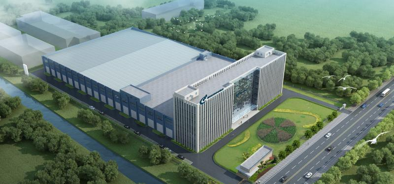
About Mikrouna
Shanghai Mikrouna Electromechanical Technology Co., Ltd
01 High tech talents
Mikrouna has a professional product research and development team, with more than 100 engineering and technical personnel, including 2 researchers (professor level senior engineers) and more than senior engineers.
02 Specialized products
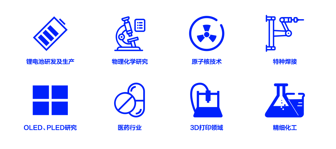
Now the production range covers isolation glove box/vacuum box products, protection/protection glove box products, laser cutting and welding machines, automation products, Internet of Things industrial intelligent products, high-end intelligent equipment and other products. These high-end equipment are widely used in lithium battery R&D and production, physical and chemical research, powder metallurgy, nuclear technology, biological pharmacy, special welding, OLED, material processing Fine chemical industry and other industries.
03 Technical achievements
It has nearly 100 patented technologies, one major national research and development project, and many high-tech achievements.
04 Worldwide service
Mikrouna products are distributed all over the world, with multiple service centers, and research and development centers in Shanghai, Hubei, and Shenyang.
Application area
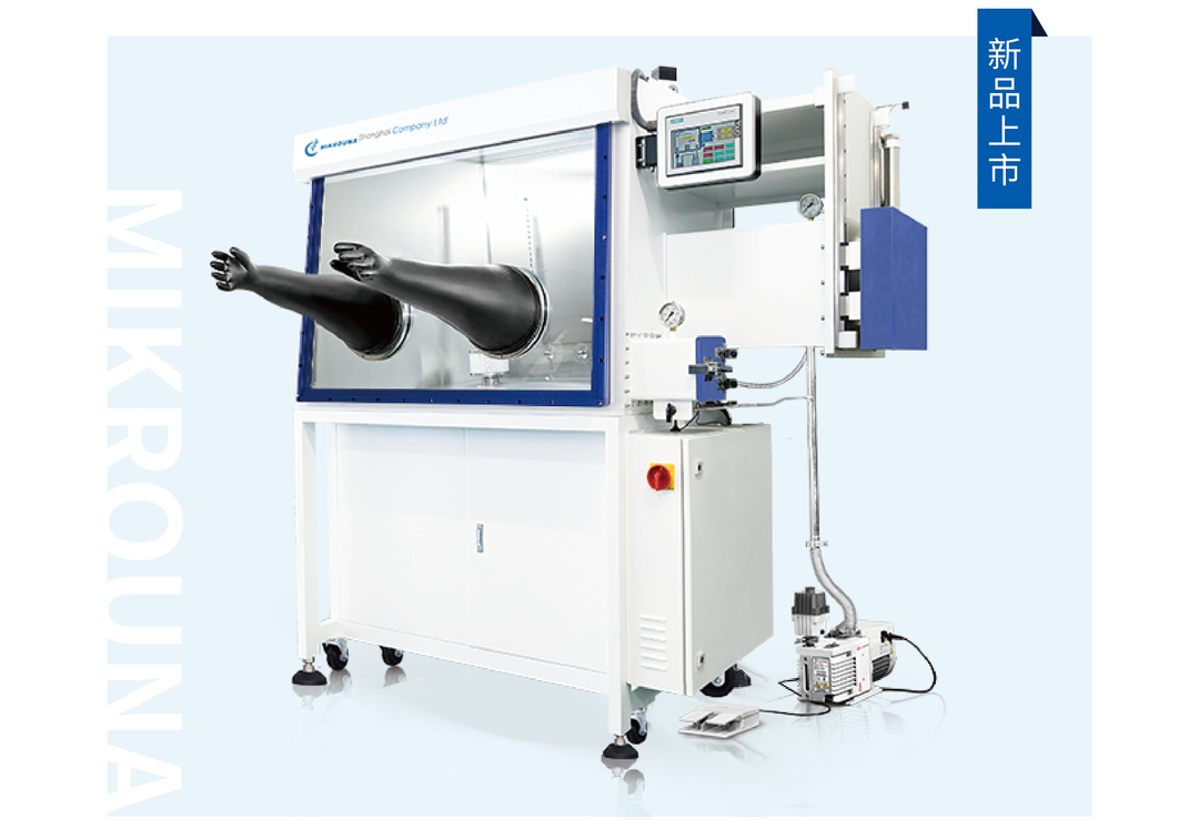
New products
O-ring vacuum sealing flange window
O-ring, "0" leakage
| "O" type "vacuum seal" flange window features | Disadvantages and Disadvantages of Traditional Windows |
|
|